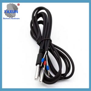
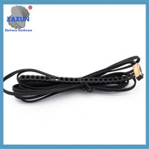
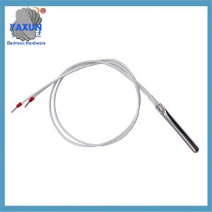
DS18B20 is a digital temperature sensor that uses a single bus timing to communicate with the host. Only 1 Wire is needed to complete the temperature data reading;
DS18B20 has a built-in 64-bit product serial number for easy identification. Multiple DS18B20 sensors can be connected to 1 Wire, and through 64-bit identity authentication, the temperature information collected from different sensors can be read separately.
Introduction to DS18B20
2.1 Main features of DS18B20
1. Fully digital temperature conversion and output.
2. Advanced single bus data communication.
3. Up to 12-bit resolution, with an accuracy of up to ±0.5 degrees Celsius.
4. The maximum working cycle at 12-bit resolution is 750 milliseconds.
5. Parasitic working mode can be selected.
6. The detection temperature range is –55° C ~+125° C (–67° F ~+257° F).
7. Built-in EEPROM, temperature limit alarm function.
8. 64-bit photolithography ROM, built-in product serial number, convenient for multi-machine connection.
9. Various packaging forms, adapt to different hardware systems.
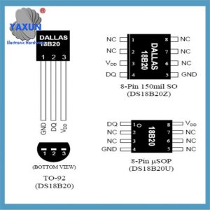
2.2 DS18B20 pin function
GND voltage ground;
DQ single data bus;
VDD power supply voltage;
NC empty pin;
2.3 DS18B20 working principle and application
DS18B20 temperature detection and digital data output are fully integrated on one chip, so it has stronger anti-interference ability. Its one working cycle can be divided into two parts, namely temperature detection and data processing.
18B20 has three forms of memory resources. They are: ROM read-only memory, used to store DS18B20ID code; the first 8 bits are single-line series code (DS18B20 code is 19H), the following 48 bits are the unique serial number of the chip; the last 8 bits are the CRC code (redundancy check) of the above 56 bits. The data is set at production and cannot be changed by the user. DS18B20 has a total of 64 bits of ROM.
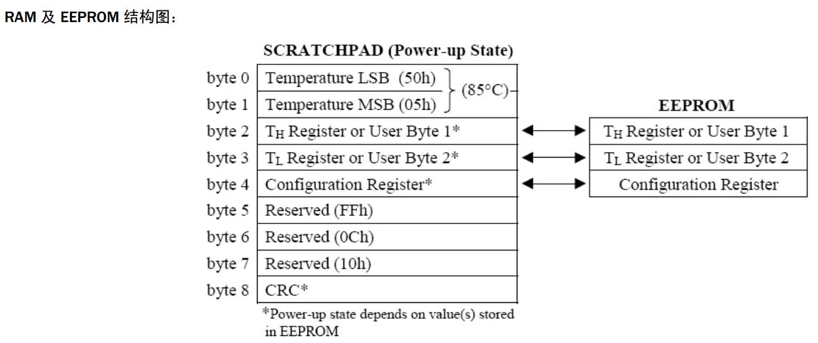
RAM data register, used for internal calculation and data access, data is lost after power failure, DS18B20 has a total of 9 bytes of RAM, each byte is 8 bits. The first and second bytes are the data value information after temperature conversion; the third and fourth bytes are the mirror image of the user’s EEPROM (commonly used for temperature alarm value storage). Its value will be refreshed when the power is reset. The fifth byte is the mirror image of the user’s third EEPROM. The 6th, 7th, and 8th bytes are count registers, which are designed to allow users to obtain higher temperature resolution. They are also temporary storage units for internal temperature conversion and calculation. The 9th byte is the CRC code of the first 8 bytes. EEPROM is a non-volatile memory used to store data that needs to be saved for a long time, upper and lower temperature alarm values, and verification data. DS18B20 has a total of 3 bits of EEPROM, and there are mirror images in RAM to facilitate user operation.
DS18B20 works in 12-bit resolution mode by default. The 12-bit data obtained after conversion is stored in two 8-bit RAMs of DS18B20 (the first two bytes). The first 5 bits in binary are sign bits. If the measured temperature is greater than 0, these 5 bits are 0. Just multiply the measured value by 0.0625 to get the actual temperature. If the temperature is less than 0, these 5 bits are 1. The measured value needs to be inverted, added by 1, and then multiplied by 0.0625 to get the actual temperature. Or use bit operation to extract temperature: the decimal places occupy the lower 4 bits, and the upper bits are integer bits (negative numbers are not considered).
2.4 DS18B20 chip ROM instruction table
1. Read ROM [33H] (the hexadecimal command word is in square brackets).
This command allows the bus controller to read the 64-bit ROM of DS18B20. This instruction can only be used when there is only one DS18B20 on the bus. If more than one is connected, data conflicts will occur during communication.
2. atch ROM [55H]
This instruction is followed by a 64-bit serial number issued by the controller. When there are multiple DS18B20s on the bus, only the chip with the same serial number as the one issued by the controller can respond, and the other chips will wait for the next reset. This instruction is suitable for single-chip and multi-chip connection.
3. Skip ROM [CCH]
This instruction makes the chip not respond to the ROM code. In the case of a single bus, this instruction can be used to save time. If this instruction is used when multiple chips are connected, data conflicts will occur, resulting in errors.
4. Search ROM [F0H]
After the chip is initialized, the search instruction allows the 64-bit ROM of all devices to be identified by elimination when multiple chips are connected to the bus.
5. Alarm Search [ECH]
In the case of multiple chips, the alarm chip search instruction only responds to chips that meet the alarm condition of temperature higher than TH or less than TL. As long as the chip is not powered off, the alarm state will be maintained until the temperature is measured again and the alarm condition is not reached.
6. Write Scratchpad [4EH]
This is the instruction to write data to RAM. The two bytes of data written subsequently will be stored at address 2 (TH of alarm RAM) and address 3 (TL of alarm RAM). The write process can be terminated by a reset signal.
7. Read Scratchpad (read data from RAM) [BEH]
This instruction will read data from RAM, starting from address 0 and up to address 9, completing the reading of the entire RAM data. The chip allows the reset signal to terminate the reading process, that is, the subsequent unnecessary bytes can be ignored to reduce the reading time.
8. Copy Scratchpad (copy RAM data to EEPROM) [48H]
This instruction stores the data in RAM into EEPROM so that the data will not be lost when power is off. Since the chip is busy with EEPROM storage processing, when the controller sends a read time slot, the bus outputs “0”, and when the storage work is completed, the bus will output “1”.
In parasitic working mode, a strong pull-up must be used immediately after this instruction is issued and maintained for at least 10MS to maintain chip operation.
9. Convert T (temperature conversion) [44H]
After receiving this instruction, the chip will perform a temperature conversion and store the converted temperature value in the 1st and 2nd addresses of RAM. Since the chip is busy with temperature conversion processing, when the controller sends a read time slot, the bus outputs “0”, and when the storage work is completed, the bus will output “1”. In parasitic working mode, a strong pull-up must be used immediately after this instruction is issued and maintained for at least 500MS to maintain chip operation.
10. Recall EEPROM (Copy the alarm value in EEPROM to RAM) [B8H]
This instruction copies the alarm value in EEPROM to the 3rd and 4th bytes in RAM. Since the chip is busy with copying processing, when the controller sends a read time slot, the bus outputs “0”, and when the storage work is completed, the bus outputs “1”. In addition, this instruction will be automatically executed when the chip is powered on and reset. In this way, the two alarm byte bits in RAM will always be the mirror image of the data in EEPROM.
11. Read Power Supply (Working Mode Switch) [B4H]
After this instruction is issued, a read time gap is issued, and the chip will return its power status word. “0” is the parasitic power state and “1” is the external power state.
2.5 DS18B20 Timing Diagram
2.5.1 DS18B20 Reset and Response Relationship Diagram
A reset must be performed before each communication. The reset time, waiting time, and response time should be strictly programmed according to the timing.
DS18B20 read and write time gap: DS18B20 data reading and writing is confirmed by the time gap processing bit and command word to exchange information.
2.5.2 Write data 0 and data 1 to DS18B20
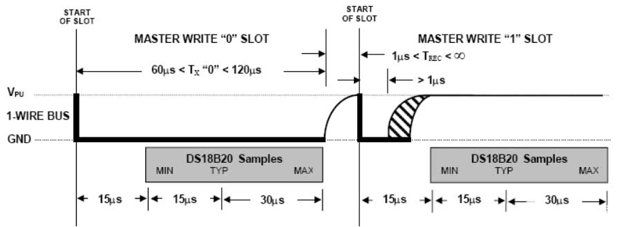
In the first 15uS of the write data time gap, the bus needs to be pulled low by the controller, and then it will be the chip sampling time for the bus data. The sampling time is 15~60uS. If the controller pulls the bus high during the sampling time, it means writing “1”, and if the controller pulls the bus low, it means writing “0”.
Each bit of transmission should have a low-level start bit of at least 15uS, and the subsequent data “0” or “1” should be completed within 45uS.
The transmission time of the entire bit should be kept at 60~120uS, otherwise the normal communication cannot be guaranteed.
Note: DS18B20 reads and writes data from the low bit.
2.5.3 Reading data 0 and data 1 from DS18B20
The sampling time of the control during the read time gap should be more accurate. During the read time gap, the host must also generate a low level of at least 1uS to indicate the start of the read time. Then, in 15uS after the bus is released, the DS18B20 will send the internal data bit. At this time, if the control finds that the bus is high, it means reading “1”, and if the bus is low, it means reading data “0”. Before reading each bit, the controller adds a start signal.
Note: The data bit must be read within 15uS of the start of the read gap to ensure correct communication.
During communication, 8 bits of “0” or “1” are used as a byte, and the reading or writing of the byte starts from the low bit.
2.5.4 Order of reading temperature once (only a single DS18B20 on the bus)
1. Send reset signal
2. Detect response signal
3. Send 0xCC
4. Send 0x44
5. Send reset signal
6. Detect response signal
7. Write 0xcc
8. Write 0xbe
9. Loop 8 times to read the low byte of temperature
10. Loop 8 times to read the high byte of temperature
11. Synthesize 16-bit temperature data and process
3. Driver code
3.1 DS18B20.c
#include “ds18b20.h”
/*
Function: DS18B20 initialization
Hardware connection: PB15
*/
void DS18B20_Init(void)
{
RCC->APB2ENR|=1<<3; //PB
GPIOB->CRH&=0x0FFFFFFF;
GPIOB->CRH|=0x30000000;
GPIOB->ODR|=1<<15; //Pull-up
}
/*
Function: Check if the DS18B20 device exists
Return value: 1 means the device does not exist 0 means the device is normal
*/
u8 DS18B20_CheckDevice(void) //Contains reset pulse, detection pulse
{
DS18B20_OUTPUT_MODE();//Initialize to output mode
DS18B20_OUT=0; //Generate reset pulse
DelayUs(750); //Generate 750us low level
DS18B20_OUT=1; //Release bus
DelayUs(15); //Wait for DS18B20 response
if(DS18B20_CleckAck())//Detect existence pulse
{
return 1;
}
return 0;
}
/*
Function: Detect existence pulse of DS18B20 device
Return value: 1 indicates error 0 indicates normal
*/
u8 DS18B20_CleckAck(void)
{
u8 cnt=0;
DS18B20_INPUT_MODE();//Initialize to input mode
while(DS18B20_IN&&cnt<200) //Wait for DS18B20 response existence pulse
{
DelayUs(1);
cnt++;
}
if(cnt>=200)return 1; //error
cnt=0;
while((!DS18B20_IN)&&cnt<240) //wait for DS18B20 to release the bus
{
DelayUs(1);
cnt++;
}
if(cnt>=240)return 1; //error
return 0;
}
/*
Function: Write a byte
First learn how to write a bit.
*/
void DS18B20_WriteByte(u8 cmd)
{
u8 i;
DS18B20_OUTPUT_MODE(); //Initialize to output mode
for(i=0;i<8;i++)
{
DS18B20_OUT=0; //Generate write time gap (write start)
DelayUs(2);
DS18B20_OUT=cmd&0x01; //Send actual data bit
DelayUs(60); //Wait for write completion
DS18B20_OUT=1; //Release the bus and prepare for the next transmission
cmd>>=1; //Continue to send the next bit of data
}
}
/*
Function: Read a byte
First learn how to read a bit.
*/
u8 DS18B20_ReadByte(void)
{
u8 i,data=0;
for(i=0;i<8;i++)
{
DS18B20_OUTPUT_MODE(); //Initialize to output mode
DS18B20_OUT=0; //Generate read time gap (read start)
DelayUs(2);
DS18B20_OUT=1; //Release bus
DS18B20_INPUT_MODE(); //Initialize to input mode
DelayUs(8); //Wait for DS18B20 data output
data>>=1; //Fill high bit with 0, default is 0
if(DS18B20_IN) data|=0x80;
DelayUs(60);
DS18B20_OUT=1; //Release bus, wait for reading next bit of data
}
return data;
}
/*
Function: Read the temperature data of DS18B20 once
Return value: the temperature data read
Considered situation: There is only one DS18B20 connected to the bus
*/
u16 DS18B20_ReadTemp(void)
{
u16 temp=0;
u8 temp_H,temp_L;
DS18B20_CheckDevice(); //Send reset pulse, detect pulse
DS18B20_WriteByte(0xCC); //Skip ROM sequence detection
DS18B20_WriteByte(0x44); //Start a temperature conversion
//Wait for temperature conversion to complete
while(DS18B20_ReadByte()!=0xFF){}
DS18B20_CheckDevice(); //Send reset pulse, detect pulse
DS18B20_WriteByte(0xCC); //Skip ROM sequence detection
DS18B20_WriteByte(0xBE); //Read temperature
temp_L=DS18B20_ReadByte(); //Read low temperature data
temp_H=DS18B20_ReadByte(); //Read high temperature data
temp=temp_L|(temp_H<<8); //Synthesized temperature
return temp;
}
3.2 DS18B20.h
#ifndef DS18B20_H
#define DS18B20_H
#include “stm32f10x.h”
#include “sys.h”
#include “delay.h”
#include “ds18b20.h”
#include “usart.h”
/*Package interface*/
//Initialize DS18B20 to input mode
#define DS18B20_INPUT_MODE() {GPIOB->CRH&=0x0FFFFFFF;GPIOB->CRH|=0x80000000;}
//Initialize DS18B20 to output mode
#define DS18B20_OUTPUT_MODE(){GPIOB->CRH&=0x0FFFFFFF;GPIOB->CRH|=0x30000000;}
//DS18B20 IO port output
#define DS18B20_OUT PBout(15)
//DS18B20 IO port input
#define DS18B20_IN PBin(15)
//Function declaration
u8 DS18B20_CleckAck(void);
u8 DS18B20_CheckDevice(void);
void DS18B20_Init(void);
u16 DS18B20_ReadTemp(void);
u8 DS18B20_ReadByte(void);
void DS18B20_WriteByte(u8 cmd);
#endif
poYBAGDYdXCAWkKMAAAAK8RNs4s030.png
3.3 Delay function
/*
Function: Delay in us
*/
void DelayUs(int us)
{
#ifdef _SYSTICK_IRQ_
int i,j;
for(i=0;iVAL=0; //CNT counter value
SysTick->LOAD=9*us; //9 means 1us
SysTick->CTRL|=1<<0; //Start timer
do
{
tmp=SysTick->CTRL; //Read status
}while((!(tmp&1<<16))&&(tmp&1<<0));
SysTick->VAL=0; //CNT counter value
SysTick->CTRL&=~(1<<0); //Turn off the timer
#endif
};i++)>
3.4 main.c Call DS18B20 to read the temperature and print it to the serial port
#include “stm32f10x.h”
#include “ds18b20.h”
u8 DS18B20_ROM[8]; //Store the 64-bit ROM code of DS18B20
int main(void)
{
u16 temp;
USARTx_Init(USART1,72,115200);//Initialization of serial port 1
DS18B20_Init(); //DS18B20 initialization
/*1. Read the 64-bit ROM code of DS18B20*/
//Send reset pulse, detect existence pulse
while(DS18B20_CheckDevice())
{
printf(“DS18B20 device does not exist!\n”);
DelayMs(500);
}
//Send the command to read the 64-bit ROM code
DS18B20_WriteByte(0x33);
//Loop read 64-bit ROM code
for(i=0;i<8;i++)
{
DS18B20_ROM[i]= DS18B20_ReadByte();
printf(“DS18B20_ROM[%d]=0x%X\n”,i,DS18B20_ROM[i]);
}
while(1)
{
/*2. Simultaneously operate all DS18B20 on the bus to start converting temperature*/
DS18B20_CheckDevice(); //Send reset pulse, detect pulse
DS18B20_WriteByte(0xCC); //Skip ROM sequence detection
DS18B20_WriteByte(0x44); //Start a temperature conversion (let all DS18B20 on the bus convert the temperature)
DelayMs(500); //Wait for all DS18B20 temperature conversions on the line to complete
/*3. Single targeted reading of the temperature of each DS18B20*/
DS18B20_CheckDevice(); //Send reset pulse, detect pulse
DS18B20_WriteByte(0x55); //Send command to match ROM
for(i=0;i<8;i++) //Send 64-bit code
{
DS18B20_WriteByte(DS18B20_ROM[i]);
}
DS18B20_WriteByte(0xBE); //Read temperature
temp=DS18B20_ReadByte(); //Read low-order temperature data
temp|=DS18B20_ReadByte()<<8; //Read high-order temperature data
printf(“temp1=%d.%d\n”,temp>>4,temp&0xF);
printf(“temp2=%f\n”,temp*0.0625);
DelayMs(500);
}
}
 English
 العربية
 Български
 粤语
粤语 中文(简体)
 中文(漢字)
 Nederlands
 Suomi
Suomi Français
 Deutsch
 Ελληνικά
 Magyar
 Italiano
 日本語
日本語 한국어
한국어 Polski
 Português
 Română
 Русский
 Slovenščina
 Español
 Svenska
 ภาษาไทย
 Türkçe
 Tiếng Việt

