DS18B20 Temperature Sensor Knowledge Introduction
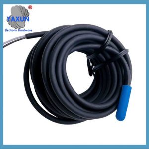
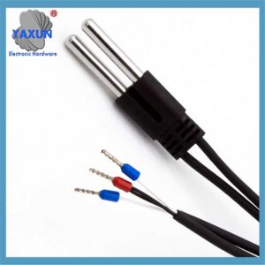
DS18B20 est un capteur de température numérique couramment utilisé. It outputs digital signals, has the characteristics of small size, faible surcharge matérielle, forte capacité anti-interférence, haute précision, and is widely used.
Introduction to DS18B20 Temperature Sensor
Technical Features:
①. Unique single-wire interface mode. When DS18B20 is connected to a microprocessor, only 1 wire is needed to realize two-way communication between the microprocessor and DS18B20.
②. Temperature measurement range -55℃~+125℃, inherent temperature measurement error 1℃.
③. Support multi-point networking function. Multiple DS18B20 can be connected in parallel on the only three wires, and a maximum of 8 can be connected in parallel to realize multi-point temperature measurement. If the number is too large, the power supply voltage will be too low, resulting in unstable signal transmission.
④. Working power supply: 3.0~5.5V/DC (data line parasitic power supply can be used).
⑤. No peripheral components are required during use.
⑥. The measurement results are transmitted serially in 9~12-bit digital form.
⑦. The diameter of the stainless steel protective tube is Φ6.
⑧. It is suitable for temperature measurement of various medium industrial pipelines of DN15~25, DN40~DN250 and equipment in narrow spaces.
⑨. Standard installation threads M10X1, M12X1.5, G1/2” are optional.
⑩. PVC cable is directly connected or German ball-type junction box is connected, which is convenient for connection with other electrical equipment.
DS18B20 read and write timing and temperature measurement principle:
DS18B20 temperature measurement principle is shown in Figure 1. The oscillation frequency of the low temperature coefficient crystal oscillator in the figure is little affected by temperature, and is used to generate a fixed frequency pulse signal to be sent to counter 1. The oscillation frequency of the high temperature coefficient crystal oscillator changes significantly with temperature, and the generated signal is used as the pulse input of counter 2. Counter 1 and the temperature register are preset to a base value corresponding to -55℃. Counter 1 subtracts the pulse signal generated by the low temperature coefficient crystal oscillator. When the preset value of counter 1 is reduced to 0, the value of the temperature register will be increased by 1, and the preset of counter 1 will be reloaded. Counter 1 restarts to count the pulse signal generated by the low temperature coefficient crystal oscillator, and the cycle continues until counter 2 counts to 0, stopping the accumulation of the temperature register value. A cette époque, the value in the temperature register is the measured temperature. The slope accumulator is used to compensate and correct the nonlinearity in the temperature measurement process, and its output is used to correct the preset value of counter 1.
Chiffre 1 is as follows:
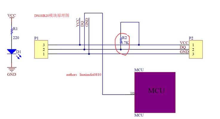
2. DS18B20 and MCU connection diagram
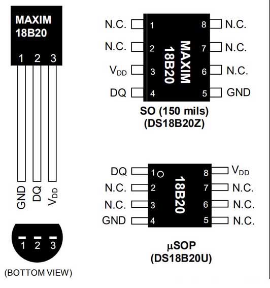
3. Définition des broches DS18B20:
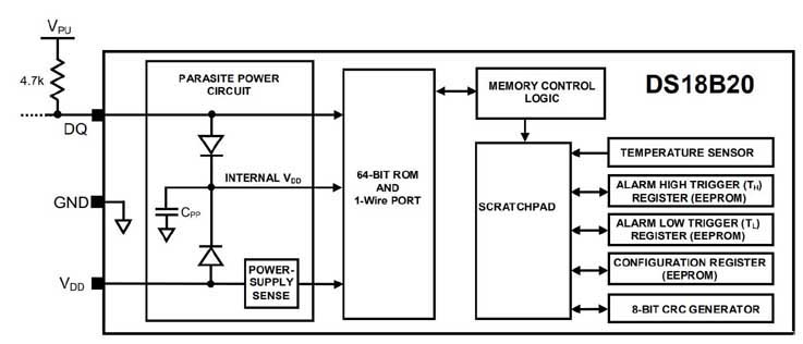
DQ: Data input/output. Open drain 1-wire interface. It can also provide power to the device when used in parasitic power mode VDD: positive power supply GND: power ground 4. DS18B20 internal analysis introduction:
The above figure shows the block diagram of DS18B20, and the 64-bit ROM stores the unique serial code of the device. The buffer memory contains 2 bytes of temperature registers that store the digital output of the temperature sensor. En outre, the buffer memory provides access to 1-byte upper and lower alarm trigger registers (TH and TL) and 1-byte configuration registers. The configuration register allows the user to set the resolution of the temperature to digital conversion to 9, 10, 11, ou 12 morceaux. ÈME, TL, and configuration registers are non-volatile (EEPROM), so they will retain data when the device is powered off. DS18B20 uses Maxim’s unique 1-wire bus protocol, which uses a control signal. The control line requires a weak pull-up resistor because all devices are connected to the bus through a 3-state or open-drain port (DQ pin in the case of the DS18B20). In this bus system the microprocessor (master) uses a unique 64-bit code for each device. Because each device has a unique code, the number of devices that can be addressed on one bus is virtually unlimited.
Temperature Register Format
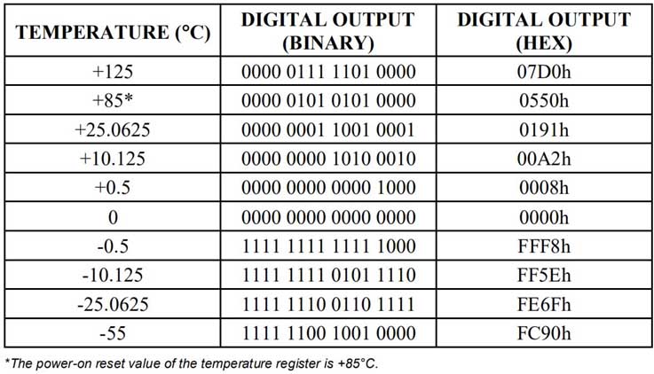
Temperature/Data Relationship
Operation Alarm Signal
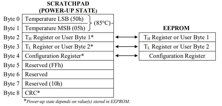
After the DS18B20 performs a temperature conversion, it compares the temperature value to the user-defined two’s complement alarm trigger value stored in the 1-byte TH and TL registers. The sign bit indicates whether the value is positive or negative: positive S=0, negative S=1. The TH and TL registers are non-volatile (EEPROM) and therefore are not volatile when the device is powered off. TH and TL can be accessed through bytes 2 et 3 of the memory.
TH and TL register format:
Schematic diagram of powering the DS18B20 using an external power supply
64-bit laser read-only memory code:
Each DS18B20 contains a unique 64-bit code stored in ROM. The least significant 8 bits of the ROM code contain the single-wire family code of the DS18B20: 28H. The next 48 bits contain a unique serial number. The most significant 8 bits contain a cyclic redundancy check (CRC) byte, which is calculated from the first 56 bits of the ROM code.
DS18B20 memory map
Configuration Register:
Chiffre 2
Byte 4 of the memory contains the configuration register, which is organized as shown in Figure 2. The user can set the conversion resolution of the DS18B20 using bits R0 and R1 here as shown in Table 2. The power-on defaults for these bits are R0 = 1 and R1 = 1 (12-bit resolution). Note that there is a direct relationship between resolution and conversion time. Bit 7 and bits 0 à 4 in the configuration register are reserved for internal use of the device and cannot be overwritten.
Tableau 2 Thermometer Resolution Configuration
CRC Generation
The CRC byte is part of the DS18B20 64-bit ROM code and is provided in the 9th byte of the scratchpad. The ROM code CRC is calculated from the first 56 bits of the ROM code and is contained in the most significant byte of the ROM. The scratchpad CRC is calculated based on the data stored in the scratchpad, so it changes when the data in the scratchpad changes. The CRC provides the bus host with a method of data verification when reading data from the DS18B20. After verifying that the data has been read correctly, the bus master must recalculate the CRC from the received data and then compare that value to the ROM code CRC (for ROM reads) or the scratchpad CRC (for scratchpad reads). If the calculated CRC matches the read CRC, the data has been received correctly. The decision to compare the CRC values and proceed is entirely at the bus master’s discretion. There is no circuitry inside the DS18B20 that will prevent the execution of a command sequence if:
The DS18B20 CRC (ROM or scratchpad) does not match the value generated by the bus master.
The equivalent polynomial function for the CRC is:
CRC = X8 + X5 + X4 + 1
The bus master can recalculate the CRC and compare it to the DS18B20’s CRC value by:
The polynomial generator is shown in Figure 3. The circuit includes a shift register and yihuo gates, and the bits of the shift register are initialized to 0. The least significant bit of the ROM code or the least significant bit of byte 0 in the scratchpad should be shifted into the shift register one at a time. After shifting in bit 56 from the ROM or the most significant bit of byte 7 from the scratchpad, the polynomial generator will contain the recalculated CRC. Suivant, the 8-bit ROM code or the CRC signal in the scratchpad DS18B20 must be shifted into the circuit. À ce point, if the recalculated CRC is correct, the shift register will be all 0s.
Chiffre 3: CRC Generator
V. Accessing the DS18B20:
The sequence for accessing the DS18B20 is as follows:
Étape 1. Initialization;
Étape 2. ROM command (followed by any necessary data exchange);
Étape 3. DS18B20 function command (followed by any necessary data exchange);
Note: This sequence is followed every time the DS18B20 is accessed, because the DS18B20 will not respond if any step in the sequence is missing or out of order. The exception to this rule is the Search ROM [F0h] and Alarm Search [ECh] commands. After issuing these two ROM commands, the host must return to step 1 in sequence.
(The above introduction is translated from the official manual)
ROM Command
1, Read ROM [33H]
2, Match ROM [55H]
3, Skip ROM [CCh]
4, Alarm Search [ECh]
DS18B20 Function Command
1, Convert Temperature [44H]
2, Write Scratchpad (Memory) [4Eh]
3, Read Scratchpad (Memory) [BEh]
4, Copy Scratchpad (Memory [48H]
5, Re-wake E2 [B8h]
6, Read Power [B4h]
(For detailed description of the above commands, see the official manual)
VI. Access DS18B20 Timing
During the initialization process, the bus master sends a reset pulse (TX) low level for at least 480µs by pulling the 1-Wire bus. Alors, the bus master releases the bus and enters the receiving mode (RX). After releasing the bus, the 5kΩ pull-up resistor pulls the 1-Wire bus high. When the DS18B20 detects this rising edge, it waits 15µs to 60µs and then sends a presence pulse by pulling the 1-Wire bus low for 60µs to 240µs.
Initialization Timing:
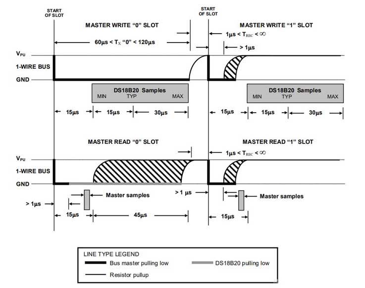
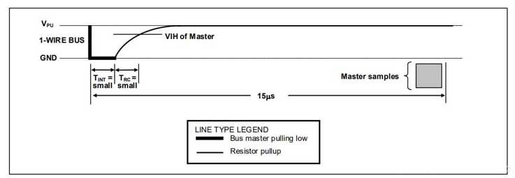
There are two types of write time slots: “Write 1” time slots and “Write 0” time slots. The bus uses a Write 1 time slot to write a logic 1 to the DS18B20 and a Write 0 time slot to write a logic 0 to the DS18B20. All write time slots must be at least 60µs in duration with a recovery time of at least 1µs between individual write time slots. Both types of write time slots are initiated by the master pulling the 1-Wire bus low (see Figure 14). To generate a Write 1 time slot, after pulling the 1-Wire bus low, the bus master must release the 1-Wire bus within 15µs. After releasing the bus, the 5kΩ pull-up resistor pulls the bus high. Generate a
Écrire 0 time slot, after pulling the 1-Wire line low, the bus master must continue to hold the bus low for the duration of the time slot (at least 60µs). The DS18B20 samples the 1-Wire bus within a window of 15µs to 60µs after the master initiates the write time slot. If the bus is high during the sampling window, un 1 is written to the DS18B20. If the line is low, un 0 is written to the DS18B20.
Note: Timeslot is a portion of the serial self-multiplexing of the time slot information dedicated to a single channel.
Chiffre 14 is as follows:
Read time slot:
The DS18B20 can only send data to the host when the host issues a read time slot. Donc, the host must generate a read time slot immediately after issuing a Read Memory Command [BEh] or a Read Power Supply [B4h] command in order for the DS18B20 to provide the required data. Alternativement, the host can generate a read time slot after issuing a Convert T [44H] or Recall E2 [B8h] command to find out the status. All read time slots must be at least 60µs in duration with a minimum recovery time of 1µs between time slots. A read time slot is initiated by the master pulling the 1-Wire bus low to hold it low for at least 1µs and then releasing the bus (see Figure 14). After the master initiates a read time slot, the DS18B20 will begin sending either 1s or 0s on the bus. The DS18B20 sends a 1 by holding the bus high and sends a 0 by pulling the bus low. When a 0 is sent, the DS18B20 releases the bus by holding the bus high. The time slot ends and the bus is pulled back to the high idle state by the pull-up resistor.
 English
 العربية
 Български
 粤语
粤语 中文(简体)
 中文(漢字)
 Nederlands
 Suomi
Suomi Français
 Deutsch
 Ελληνικά
 Magyar
 Italiano
 日本語
日本語 한국어
한국어 Polski
 Português
 Română
 Русский
 Slovenščina
 Español
 Svenska
 ภาษาไทย
 Türkçe
 Tiếng Việt

