Comparison between PT100 temperatuursensor probe and DS18B20 module
1) Basisprincipe van signaalverwerving
① De weerstand van PT100 verandert evenredig met de temperatuur (Hoe hoger de temperatuur, Hoe groter de weerstand), Maar de weerstandsverandering is erg klein, over 0.385 Oh / rang;
② The temperature measurement range of PT100 is -200℃ -200℃, and at 0℃, the resistance is exactly equal to 100 Oh;
③ The working current of PT100 should be less than 5 mA;
④ Although the resistance of PT100 changes proportionally with the temperature, its change rate (dat is, K value K value K value) is different in different temperature ranges.
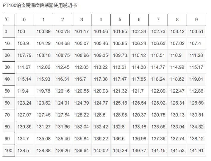
2) PT100 Temperatuurweerstand Wijziging Tabel
3. PT100 drive circuit
1) Through the voltage division method, AD collects PT100 voltage to obtain resistance value to calculate temperature
The resistance value of PT100 in water at room temperature (25℃25℃25℃) is about 109.89 Oh.
The microcontroller outputs 3.3V voltage, and the voltage divided by PT100 is approximately:
109.89 ∗ 0.005 = 0.54945 V
The AD value converted according to the AD conversion formula is approximately:
0.54945 / 3.3 ∗ 4096 = 681.98 ≈ 682
When the temperature rises by one degree, assuming that the resistance of PT100 just rises by 0.385 Oh, the change value of the voltage divided is approximately equal to:
0.385 ∗ 0.005 = 0.001925 V
The AD value converted according to the AD conversion formula is approximately:
0.001925 / 3.3 ∗ 4096 = 2.39 ≈ 2
In the experiment, it was found that due to the unstable 3.3V voltage of the stm32 power supply, the ADC collected PT100 voltage fluctuations and the voltage division error was large. The optimization solution is to design a constant current source circuit. By collecting the voltage of PT100 and the current of the constant current source, the resistance of PT100 can be obtained, and then the temperature value can be obtained.
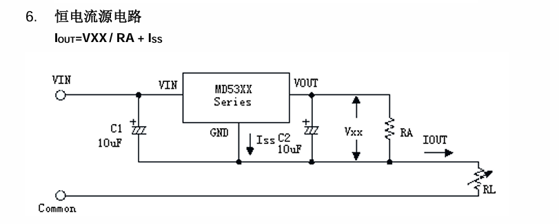
2) Constant current source circuit based on LDO regulator (MD5333)
There are many driving circuits for testing PT100 on the Internet, such as DC bridge circuit, constant current source circuit based on operational amplifier, enz. The author also spent a lot of time in selecting the driving circuit, considering the difficulty of making the board and the number of components, and finally chose the constant current source circuit based on LDO regulator (MD5333). The circuit diagram is as follows:
At this point, the hardware selection has been basically completed. The development board used is the Zhengdian Atom F10ZET6 Elite Board
DS18B20 module
In order to test the real-time temperature and PT100 temperature comparison, the DS18B20 module is added for calibration comparison test
1) Introduction to DS18B20
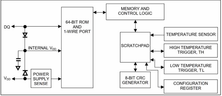
DS18B20 is a single-bus temperature sensor with a test temperature range of -55~+125℃ and an accuracy of ±0.5℃. The field temperature is directly transmitted in a single-bus digital manner, which greatly improves the anti-interference ability of the system. It can directly read the measured temperature, and can realize a 9~12-bit digital value reading method through simple programming according to actual requirements. Its operating voltage range is 3~5.5V, and it uses a variety of packaging forms, making the system setting flexible and convenient. The set resolution and the alarm temperature set by the user are stored in the EEPROM and are still saved after power failure.
2) Introduction to DS18B20 working timing
All single-bus devices require strict signal timing to ensure data integrity. DS18B20 has 6 signal types: reset puls, response pulse, schrijven 0, schrijven 1, lezen 0 and read 1. All these signals, except the response pulse, are synchronous signals sent by the host. And all commands and data are sent with the low bit of the byte first.
① Reset pulse and response pulse
All communications on the single bus start with an initialization sequence. The host outputs a low level and keeps the low level for at least 480us to generate a reset pulse. Then the host releases the bus, and the 4.7K pull-up resistor pulls the single bus high, with a delay time of 15~60us, and enters the receiving mode (Rx). Then DS18B20 pulls the bus low for 60~240us to generate a low-level response pulse.
② Write timing
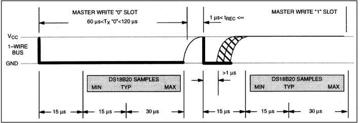
The write timing includes write 0 timing and write 1 timing. All write timings require at least 60us, and at least 1us recovery time is required between two independent write timings. Both write timings start with the host pulling down the bus. Write 1 timing: the host outputs a low level, delays for 2us, and then releases the bus, delaying 60us. Write 0 timing: the host outputs a low level, delays for 60us, and then releases the bus with a delay of 2us.
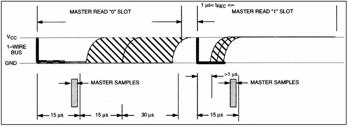
③ Read timing
Single-bus devices transmit data to the host only when the host issues a read timing. Daarom, after the host issues a read data command, a read timing must be generated immediately so that the slave can transmit data. All read timings require at least 60us, and at least 1us recovery time is required between two independent read timings. Each read timing is initiated by the host, which pulls down the bus for at least 1us. The host must release the bus during the read timing and sample the bus status within 15us after the timing starts. The typical read timing process is: the host outputs a low level delay of 2us, then the host switches to input mode delay of 12us, then reads the current level of the single bus, and then delays 50us.
After understanding the single bus timing, let’s take a look at the typical temperature reading process of DS18B20. The typical temperature reading process of DS18B20 is: reset → send SKIPROM (0xCC) → send start conversion command (0x44) → delay → reset → send SKIPROM command (0xCC) → send memory command (0xBE) → read two bytes of data (d.w.z. temperatuur) continuously → end.
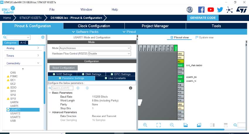
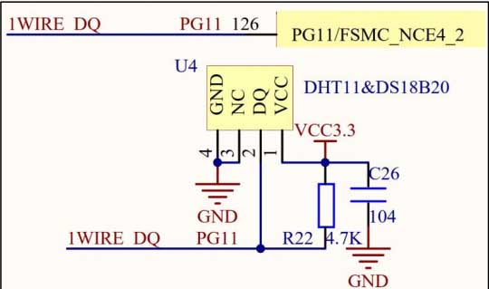
3) Schematic diagram and CUBEMAX configuration
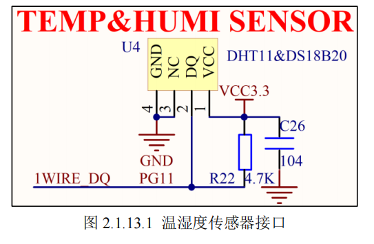
From the schematic diagram, it can be seen that DS18B20 is enabled by PG11 port to open the serial port to print temperature information
4) Code part
The code part transplants the ds18b20 library of Zhengdian Atom and makes slight modifications
#ifndef __DS18B20_H
#define __DS18B20_H
#include “tim.h”
/***********************************************************************************/
/* DS18B20 pin definition */
#define DS18B20_DQ_GPIO_PORT GPIOG
#define DS18B20_DQ_GPIO_PIN GPIO_PIN_11
#define DS18B20_DQ_GPIO_CLK_ENABLE() Doen{ __HAL_RCC_GPIOG_CLK_ENABLE(); }terwijl(0) /* PG port clock enable */
/**********************************************************************************************/
/* IO operation function */
#define DS18B20_DQ_OUT(X) Doen{ X ? \
HAL_GPIO_WritePin(DS18B20_DQ_GPIO_PORT, DS18B20_DQ_GPIO_PIN, GPIO_PIN_SET) : \
HAL_GPIO_WritePin(DS18B20_DQ_GPIO_PORT, DS18B20_DQ_GPIO_PIN, GPIO_PIN_RESET); \
}terwijl(0) /* Data port output */
#define DS18B20_DQ_IN HAL_GPIO_ReadPin(DS18B20_DQ_GPIO_PORT, DS18B20_DQ_GPIO_PIN) /* Data port input */
uint8_t ds18b20_init(void); /* Initialize DS18B20 */
uint8_t ds18b20_check(void); /* Check if DS18B20 exists */
short ds18b20_get_temperature(void);/* Get temperature */
#endif
5. Infrared remote control module
1) Wireless module coding protocol
The widely used coding methods for infrared remote control are: NEC protocol of PWM (pulse width modulation) and RC-5 protocol of Philips PPM (pulse position modulation). The remote control that comes with the development board uses the NEC protocol, which has the following features:
1. 8-bit address and 8-bit instruction length;
2. Address and command are transmitted twice (to ensure reliability);
3. PWM pulse position modulation, with the duty cycle of the transmitted infrared carrier representing “0” En “1”;
4. The carrier frequency is 38Khz;
5. The bit time is 1.125ms or 2.25ms;
In the NEC protocol, how to set the data in the protocol to ‘0’ or ‘1’? Hier, the infrared receiver and infrared transmitter are separated.
Infrared transmitter: Send protocol data ‘0’ = 560us of carrier signal transmission + 560us of no carrier signal transmission
Send protocol data ‘1’ = 560us of carrier signal transmission + 1680us of no carrier signal transmission
The bit definition of infrared transmitter is shown in the figure below
Infrared receiver: Receive protocol data ‘0’ = 560us low level + 560us high level
Receive protocol data ‘1’ = 560us low level + 1680us high level
The data format of NEC remote control command is: synchronization terminal, address code, address inverse code, control code, control inverse code. The synchronization code consists of a 9ms low level and a 4.5ms high level. The address code, address inverse code, control code, and control inverse code are all 8-bit data formats. They are sent in the order of low bit first and high bit last. The inverse code is used to increase the reliability of transmission.
Daarom, input capture can be used to measure the pulse width of the high level to achieve remote control decoding.
2) Schematic diagram and CUBEMAX configuration
From the schematic diagram, we can see that the wireless module is enabled through the PB9 pin and collects through the 4 channels of TIM4:
The default pin of TIM4_CH4 is not PB9, so it needs to be set manually, and the interrupt setting is turned on at the same time
3) Code part
Capture the rising edge through the tim callback function
Op dit moment, the decoded signal can be obtained:
Op dit moment, the data is more complex and can be slightly processed:
The effect is as follows:
The last two digits are the decoded and its inverse code. Op dit moment, it can be defined as a macro to adjust the temperature threshold:
The effect is as follows:
Infrared part code:
/* USER CODE BEGIN Header */
/**
******************************************************************************
* @file : main.c
* @brief : Main program body
******************************************************************************
* @attention
*
* <h2><center>© Copyright (C) 2024 STMicroelectronics.
* All rights reserved.</center></h2>
*
* This software component is licensed by ST under BSD 3-Clause license,
* de “License”; You may not use this file except in compliance with the
* License. You may obtain a copy of the License at:
* opensource.org/licenses/BSD-3-Clause
*
******************************************************************************
*/
/* USER CODE END Header */
/* Inclusief ——————————————————————*/
#include “main.h”
#include “tim.h”
#include “usart.h”
#include “gpio.h”
/* Private includes ———————————————————-*/
/* USER CODE BEGIN Includes */
#include “stdio.h”
#include “string.h”
#define MAXUP 157
#define MAXDOWN 87
#define MINUP 221
#define MINDOWN 61
/* USER CODE END Includes */
/* Private typedef ———————————————————–*/
/* USER CODE BEGIN PTD */
/* USER CODE END PTD */
/* Private define ————————————————————*/
/* USER CODE BEGIN PD */
/* USER CODE END PD */
/* Private macro ————————————————————-*/
/* USER CODE BEGIN PM */
/* USER CODE END PM */
/* Private variables ———————————————————*/
/* USER CODE BEGIN PV */
uint32_t upCount=0;
uint16_t ValueUp=0;
uint16_t ValueDown=0;
uint8_t isUpCapt=1;
uint16_t width=0;
uint16_t buffer[128]={0};
uint16_t bufferId=0;
uint8_t rcvFalg=0;
/* USER CODE END PV */
/* Private function prototypes ———————————————–*/
void SystemClock_Config(void);
/* USER CODE BEGIN PFP */
/* USER CODE END PFP */
/* Private user code ———————————————————*/
/* USER CODE BEGIN 0 */
void HAL_TIM_PeriodElapsedCallback(TIM_HandleTypeDef *htim)
{
upCount++;
}
void HAL_TIM_IC_CaptureCallback(TIM_HandleTypeDef *htim)
{
als(isUpCapt)//If it is rising edge capture
{
ValueUp=HAL_TIM_ReadCapturedValue(htim,TIM_CHANNEL_4);
isUpCapt=0;
__HAL_TIM_SET_CAPTUREPOLARITY(htim,TIM_CHANNEL_4,TIM_ICPOLARITY_FALLING);
upCount=0;
}
else{
ValueDown=HAL_TIM_ReadCapturedValue(htim,TIM_CHANNEL_4);
isUpCapt=1;
__HAL_TIM_SET_CAPTUREPOLARITY(htim,TIM_CHANNEL_4,TIM_ICPOLARITY_RISING);
width=ValueDown+upCount*65536-ValueUp;
als(width>4400&&width<4600)
{
bufferId=0;
buffer[bufferId++]=width;
}
else if(bufferId>0)
{
buffer[bufferId++]=width;
als(bufferId>32)
{
rcvFalg=1;
bufferId=0;
}
}
}
}
void bitBuffer2num(char num[])
{
num[0]=0;
num[1]=0;
num[2]=0;
num[3]=0;
for(int i=0;i<32;i++)
{
als(buffer[i+1]<1000)
{
num[i/8]=num[i/8]<<1;
}
else
{
num[i/8]=num[i/8]<<1;
num[i/8]|=0x01;
}
}
}
/* USER CODE END 0 */
/**
* @brief The application entry point.
* @retval int
*/
int main(void)
{
/* USER CODE BEGIN 1 */
char printbuff[128]={0};
char num[4]={0};
char key=0;
/* USER CODE END 1 */
/* MCU Configuration——————————————————–*/
/* Reset of all peripherals, Initializes the Flash interface and the Systick. */
HAL_Init();
/* USER CODE BEGIN Init */
/* USER CODE END Init */
/* Configure the system clock */
SystemClock_Config();
/* USER CODE BEGIN SysInit */
/* USER CODE END SysInit */
/* Initialize all configured peripherals */
MX_GPIO_Init();
MX_TIM4_Init();
MX_USART1_UART_Init();
/* USER CODE BEGIN 2 */
/* USER CODE END 2 */
/* Infinite loop */
/* USER CODE BEGIN WHILE */
HAL_GPIO_TogglePin(LED0_GPIO_Port,LED0_Pin);
HAL_TIM_Base_Start_IT(&htim4);//Timer update generates an interrupt
HAL_TIM_IC_Start_IT(&htim4,TIM_CHANNEL_4);//
terwijl (1)
{
als(rcvFalg)
{
for(int i=0;i<4;i++)
{
bitBuffer2num(num);
sprintf(printbuff,”0x%02x “,num[i]);
HAL_UART_Transmit(&huart1,printbuff,strlen(printbuff),HAL_MAX_DELAY);
}
// sprintf(printbuff,”%u “,buffer[i]);
// HAL_UART_Transmit(&huart1,printbuff,strlen(printbuff),HAL_MAX_DELAY);
// }
HAL_UART_Transmit(&huart1,”\r\n”,2,HAL_MAX_DELAY);
rcvFalg=0;
}
printf(“%d\r\n”,num[3]);
als(num[3]==157)
{
printf(“111111\r\n”);
}
HAL_Delay(1000);
/* USER CODE END WHILE */
/* USER CODE BEGIN 3 */
}
/* USER CODE END 3 */
}
/**
* @brief System Clock Configuration
* @retval None
*/
void SystemClock_Config(void)
{
RCC_OscInitTypeDef RCC_OscInitStruct = {0};
RCC_ClkInitTypeDef RCC_ClkInitStruct = {0};
 English
 العربية
 Български
 粤语
粤语 中文(简体)
 中文(漢字)
 Nederlands
 Suomi
Suomi Français
 Deutsch
 Ελληνικά
 Magyar
 Italiano
 日本語
日本語 한국어
한국어 Polski
 Português
 Română
 Русский
 Slovenščina
 Español
 Svenska
 ภาษาไทย
 Türkçe
 Tiếng Việt

