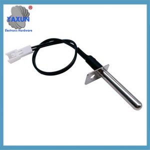
DS18B20 is a 1-wire digital temperature sensor produced by DALLAS, with a 3-pin TO-92 small package. The temperature measurement range is -55℃~+125℃, and it can be programmed to 9-bit~12-bit A/D conversion accuracy. The temperature measurement resolution can reach 0.0625℃, and the measured temperature is serially output in the form of a 16-bit digital quantity with sign extension. Its working power supply can be introduced at the remote end or generated by parasitic power supply. Multiple DS18B20s can be connected in parallel to 3 หรือ 2 lines. The CPU only needs one port line to communicate with many DS18B20s, occupying fewer ports of the microprocessor, which can save a lot of leads and logic circuits. The above characteristics make DS18B20 very suitable for long-distance multi-point temperature detection systems.
2. Internal structure of DS18B20 ds18b20 circuit diagram
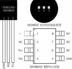
The internal structure of DS18B20 is shown in Figure 1, which mainly consists of 4 parts: 64-bit ROM, เซ็นเซอร์อุณหภูมิ, non-volatile temperature alarm triggers TH and TL, and configuration registers. The pin arrangement of DS18B20 is shown in Figure 2. DQ คือเทอร์มินัลอินพุต/เอาต์พุตสัญญาณดิจิตอล; GND เป็นแหล่งพลังงาน; VDD เป็นเทอร์มินัลอินพุตแหล่งจ่ายไฟภายนอก (grounded in parasitic power wiring mode, see Figure 4).
The 64-bit serial number in the ROM is photoetched before leaving the factory. It can be regarded as the address sequence code of the DS18B20. The 64-bit serial number of each DS18B20 is different. The cyclic redundancy check code (CRC=X8+X5+X4+1) of the 64-bit ROM is arranged. The role of ROM is to make each DS18B20 different, เพื่อให้ DS18B20 หลายตัวสามารถเชื่อมต่อกับรถบัสหนึ่งคัน.
รูป 1, internal structure of DS18B20
The temperature sensor in DS18B20 completes the temperature measurement, which is provided in the form of 16-bit sign-extended binary complement readings, expressed in the form of 0.0625℃/LSB, โดยที่ s เป็นบิตสัญญาณ. ตัวอย่างเช่น, เอาต์พุตดิจิตอล +125 ℃คือ 07d0h, เอาต์พุตดิจิตอล +25.0625 ℃คือ 0191h, the digital output of -25.0625℃ is FF6FH, และเอาต์พุตดิจิตอล -55 ℃คือ FC90H.
23
22
21
20
2-1
2-2
2-3
2-4
Temperature value low byte
MSBLSB
ส
ส
ส
ส
ส
22
25
24
Temperature value high byte
The high and low temperature alarm triggers TH and TL, and the configuration register are composed of one byte of EEPROM. A memory function command can be used to write to TH, TL, or the configuration register. The format of the configuration register is as follows:
0
R1
R0
1
1
1
1
1
MSBLSB
R1 and R0 determine the number of digits of precision for temperature conversion: R1R0 = “00”, 9-bit precision, maximum conversion time is 93.75ms; R1R0 = “01”, 10-bit precision, maximum conversion time is 187.5ms. R1R0 = “10”, 11-bit precision, maximum conversion time is 375ms. R1R0 = “11”, 12-bit precision, maximum conversion time is 750ms. The default is 12-bit precision when not programmed.
The high-speed register is a 9-byte memory. The first two bytes contain the digital information of the measured temperature; the 3rd, 4th, and 5th bytes are temporary copies of TH, TL, and configuration registers, ตามลำดับ, and are refreshed every time a power-on reset occurs; the 6th, 7th, and 8th bytes are not used and are represented as all logic 1s; the 9th byte reads the CRC code of all the previous 8 bytes, which can be used to ensure correct communication.
3. DS18B20 working sequence
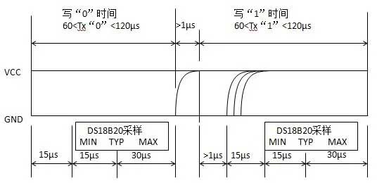
The first-line working protocol flow of DS18B20 is: initialization → ROM operation instruction → memory operation instruction → data transmission. Its working sequence includes initialization sequence, write sequence and read sequence, as shown in Figure 3 (อัน) (ข) (C).
(อัน) Initialization sequence
(C) Read sequence
รูป 3, DS18B20 working sequence diagram
4. Typical interface design of DS18B20 and single-chip microcomputer
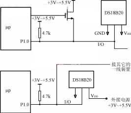
รูป 4 takes the MCS-51 series single-chip microcomputer as an example to draw the typical connection between DS18B20 and microprocessor. In Figure 4 (อัน), DS18B20 adopts parasitic power supply mode, and its VDD and GND terminals are grounded. In Figure 4 (ข), DS18B20 adopts external power supply mode, and its VDD terminal is powered by 3V~5.5V power supply.
อัน) Parasitic power supply working mode
(ข) External power supply working mode
รูป 4 Typical connection diagram of DS18B20 and microprocessor
Assuming that the crystal frequency used by the single-chip microcomputer system is 12MHz, three subroutines are written according to the initialization timing, write timing and read timing of DS18B20: INIT is the initialization subroutine; WRITE is the write (command or data) subroutine; READ is the read data subroutine. All data reading and writing start from the lowest bit.
DATEQUP1.0
……
INIT:CLREA
INI10:SETBDAT
MOVR2,#200
INI11:CLRDAT
DJNZR2,INI11; The host sends a reset pulse for 3μs×200=600μs
SETBDAT; The host releases the bus, and the port line is changed to input
MOVR2,#30
IN12:DJNZR2,INI12; DS18B20 waits for 2μs×30=60μs
CLRC
ORLC,DAT; Is the DS18B20 data line low (pulse exists)?
JCINI10; DS18B20 is not ready, re-initialize
MOVR6, #80
INI13: ORLC, DAT
JCINI14; DS18B20 data line goes high, initialization is successful
DJNZR6, INI13; data line low level can last for 3μs × 80 = 240μs
SJMPINI10; initialization failed, restart
INI14: MOVR2, #240
IN15: DJNZR2, INI15; DS18B20 responds for at least 2μs × 240 - 48 0μs
RET
;-------------------------
WRITE:CLREA
MOVR3,#8;Loop 8 ครั้ง, write a byte
WR11:SETBDAT
MOVR4,#8
RRCA;Write bit moves from A to CY
CLRDAT
WR12:DJNZR4,WR12
;Wait 16μs
MOVDAT,ค;Command word is sent to DS18B20 bit by bit
MOVR4,#20
WR13:DJNZR4,WR1 3
; Ensure that the write process lasts for 60μs
DJNZR3,WR11
; Continue before sending a byte
SETBDAT
RET
;------------------------
READ:CLREA
MOVR6,#8; Loop 8 ครั้ง, read a byte
RD11:CLRDAT
MOVR4,#4
NOP; Low level lasts for 2μs
SETBDAT; Set the port line to input
RD12:DJNZR4,RD12
; Wait for 8μs
MOVC,DA T
;The host reads the data of DS18B20 bit by bit
RRCA;The read data is moved to A
MOVR5,#30
RD13:DJNZR5,RD13
;Ensure that the reading process lasts 60μs
DJNZR6,RD11
;After reading a byte of data, store it in A
SETBDAT
RET
;-------------------------
The host must go through three steps to control DS18B20 to complete temperature conversion: initialization, ROM operation instructions, and memory operation instructions. DS18B20 must be started to start conversion before reading the temperature conversion value. Assuming that only one chip is connected to one line, the default 12-bit conversion accuracy is used, and an external power supply is used, a subroutine GETWD can be written to complete a conversion and read the temperature value.
GETWD:LCALLINIT
MOVA,#0CCH
LCALLWRITE; send skip ROM command
MOVA,#44H
LCALLWRITE; send start conversion command
LCALLINIT
MOVA,#0CCH; send skip ROM command
LCALLWRITE
MOVA,#0BEH; send read memory command
LCALLWRITE
LCALLREAD
MOVWDLSB,ก
; send low byte of temperature value to WDLSB
LCALLREAD
MOVWDMSB,ก
; send high byte of temperature value to WDMSB
RET
……
The high byte of temperature value read by subroutine GETWD is sent to WDMSB unit, and the low byte is sent to WDLSB unit. Then according to the representation format of temperature value byte and its sign bit, the actual temperature value can be obtained through simple transformation.
If multiple DS18B20 are connected on one line, parasitic power supply connection mode is adopted, conversion accuracy configuration, high and low limit alarm, ฯลฯ. are required. Then the writing of subroutine GETWD will be more complicated. Due to space limitations, this section will not be described in detail. Please refer to the relevant content.
We have successfully applied DS18B20 to the “household heating bath” control system we developed. Its fast conversion speed, high conversion accuracy, and simple interface with the microprocessor have brought great convenience to hardware design work, effectively reducing costs and shortening development cycles.
 English
 العربية
 Български
 粤语
粤语 中文(简体)
 中文(漢字)
 Nederlands
 Suomi
Suomi Français
 Deutsch
 Ελληνικά
 Magyar
 Italiano
 日本語
日本語 한국어
한국어 Polski
 Português
 Română
 Русский
 Slovenščina
 Español
 Svenska
 ภาษาไทย
 Türkçe
 Tiếng Việt


